With recent advances in the market, Ceramic PCBs have become a more viable option for PCB designers. With the continuing requirements for miniaturisation, microelectronics and high-power packages, the need for substrates capable of withstanding high operating temperatures, whilst offering outstanding thermal performance is a must. Semiconductors from materials such as Silicon Carbide and Gallium Nitride operate at high temperatures meaning associated circuits need to be ceramic. Ceramic Interposers are also becoming popular for thermal management and when a hermetic package is required where no moisture can be tolerated and no outgassing materials can be used.
Ceramics are also used for high frequency applications due to low signal loss and as well as resisting UV they are chemical resistant, have no outgassing and are completely water resistant.
Ceramics have been widely used in electronics/electronic components for years due to their thermal, and mechanical advantages. With recent advances in technology and manufacturing capabilities, they are now replacing entire PCBs.
Since their introduction, Ceramic PCBs have received enormous attention from the industry as an effective solution to a range of electronic issues. The superior Thermal Conductivity of ceramics with low signal loss for high frequency being the leading reasons that more and more industries are turning to ceramics for their PCB design.
Ceramic PCBs are used in a variety of high-temperature and high-frequency applications. Some examples include:
Aerospace and defence systems: Ceramic PCBs are used in missile guidance systems, radar systems, and other high-performance military equipment due to their ability to withstand extreme temperatures and high levels of radiation.
Automotive electronics: Ceramic PCBs are used in engine control systems, powertrain systems, and other high-temperature applications in automobiles.
Medical devices: Ceramic PCBs are used in imaging equipment, such as CT scanners, MRI machines, and X-ray machines, as well as other medical devices that require high-temperature and high-frequency operation.
Power electronics: Ceramic PCBs are used in power inverters, power supplies, and other high-power electronic devices due to their excellent thermal conductivity and high-frequency capabilities.
Industrial control systems: Ceramic PCBs are used in industrial control systems, such as temperature controllers, pressure sensors, and other industrial automation equipment, due to their high-temperature and high-frequency capabilities.
Wireless communication: Ceramic PCBs are used in wireless communication devices such as base stations, repeaters, and other RF devices due to their excellent heat dissipation and high-frequency capabilities.
Advantages Over Other Technologies
Heat dissipation is the key advantage that Ceramic has over more conventional materials such as FR4 and Metal Clad PCBs. With components being placed directly on the boards, and no isolation layer, the flow of heat through the boards is far more efficient. Depending on the material chosen, the Thermal Conductivity values range from 24-180W/mK.
In addition to this, Ceramic material can withstand high operating temperatures (over 800°C) and has a very low CTE (Coefficient of Thermal Expansion), allowing for additional compatibility options for circuit design.
Full list of advantages:
Direct Plated Copper (DPC)
DPC is a recent development in the field of Ceramic Substrate PCBs and was the breakthrough that made ceramics much more viable to designers. DPC involves vacuum sputtering under high temperature and pressure conditions to plate the copper to the substrate. The addition of a thin titanium layer acts as a bonding interface between the copper and ceramic layers. During this part of the process a very thin layer of copper is deposited coating the Ceramic substrate and it is also deposited in any pre-drilled holes. The circuit is then formed with etching . The thin copper allows very fine tracks and reduced undercutting. Panels are then plated up to the required end copper thickness ranging from 10um (≈ 1/3oz) to 140um (4oz). DPC enables the circuit to incorporate plated or filled vias. Normal PTH methods do not produce reliable results on ceramics and therefore DPC must be used if a double sided PTH board is required. With DPC it is also possible to produce a circuit with different thicknesses of copper in selected areas. You could therefore have a control section and a power section on the same layer.
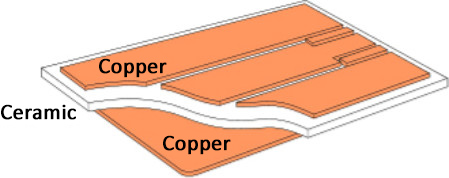
Direct Bonded Copper (DBC)
With DBC the copper is bonded to the Ceramic substrate on one or both sides using a high-temperature oxidation process. It offers options of heavy copper thickness - 140um (4oz)-350um (10oz). The copper and substrate are heated in an atmosphere of nitrogen containing about 30 ppm of oxygen; under these conditions, a copper-oxygen eutectic forms which bonds successfully both to copper and the oxides used as substrates. With DBC the copper layers can then be etched using standard PCB technology to form the required circuit. Conventional PTH processing is not suitable for ceramics and therefore only DPC is used for through hole plating.
Active Metal Brazing (AMB)
AMB is the latest development in ceramic substrates. Unlike DBC Active Metal Brazing forms the substrates without metallisation. Under a high temperature vacuum the copper is joined (brazed) direct to the ceramic base. This offers a high reliability substrate with unique heat dissipation. The brazing technology also enables copper weights of up to 800µm on thin ceramic substrates. These Heavy Copper materials make AMB ideal for Power Electronics.
Ceramic Substrate Options
Ceramic Material Specifications
| Property | Unit | Al2O3 (96%) | Al2O3 (99.6%) | AlN | SiN |
|---|---|---|---|---|---|
| Thermal Conductivity | W/mK | 24 | 29 | 180 | 85 |
| Coefficient of Thermal Expansion (CTE) | x 10¯6/K | 6.7 | 6.8 | 4.6 | 2.6 |
| Dielectric Constant | - | 9.8 | 9.9 | 9 | 9 |
| Signal Loss | x 10¯3 | 0.2 | 0.2 | 0.2 | 0.2 |
| Light Reflectivity | % | 70/85 | 75 | 35 | - |
| Dielectric Strength | KV/mm | ≥15 | ≥15 | ≥15 | ≥15 |
| Rupture Strength | Mpa | 400 | 550 | 450 | 800 |
| Max Operating Temperature | Al2O3 (96%) | Al2O3 (99.6%) | AlN | SiN |
|---|---|---|---|---|
| Substrate | 850°C | 850°C | 850°C | 850°C |
| Cu Conductor | 300°C | 300°C | 300°C | 300°C |
| Solder Resist* | < 300°C | < 300°C | < 300°C | < 300°C |
*Solder Resist - 130°C is maximum long term exposure. As a minimum, all Solder Resists used pass IPC thermal stress test; 3 times, 288°, 10 seconds.
Highlighted in the table are some of the extreme values that suit each material for different applications -
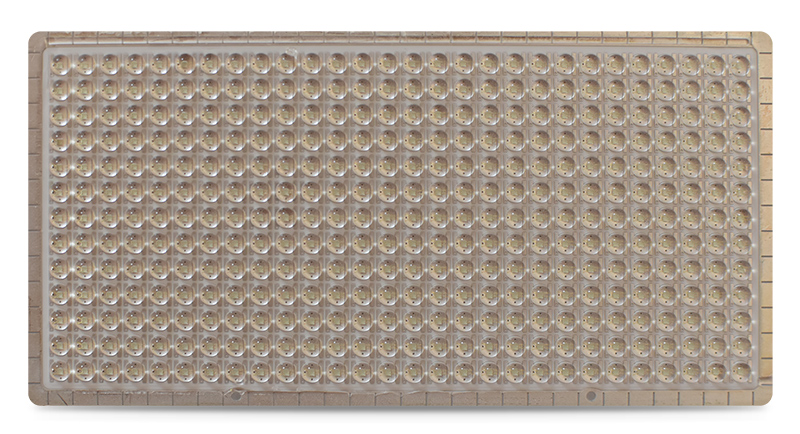 Populated with LEDs
 Silver Paste Conductor with ENIG Surface Treatment
 Immersion Tin Panel
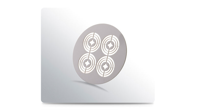 Alumina Oxide Al2O3
 Direct Bonded Copper
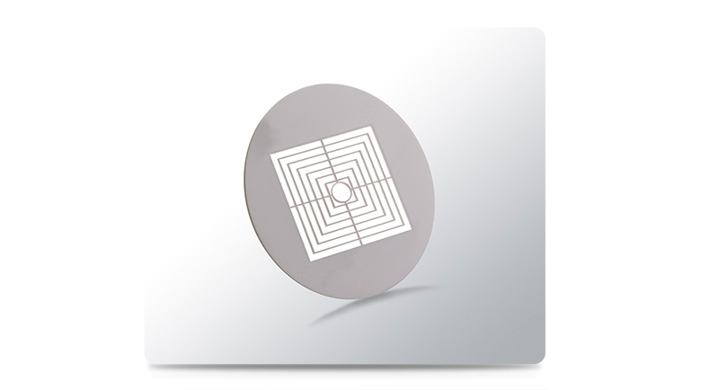 Alumina Oxide Al2O3
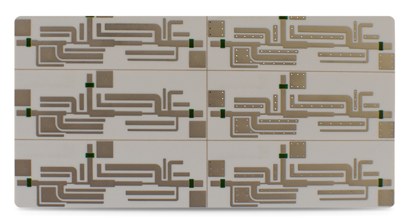
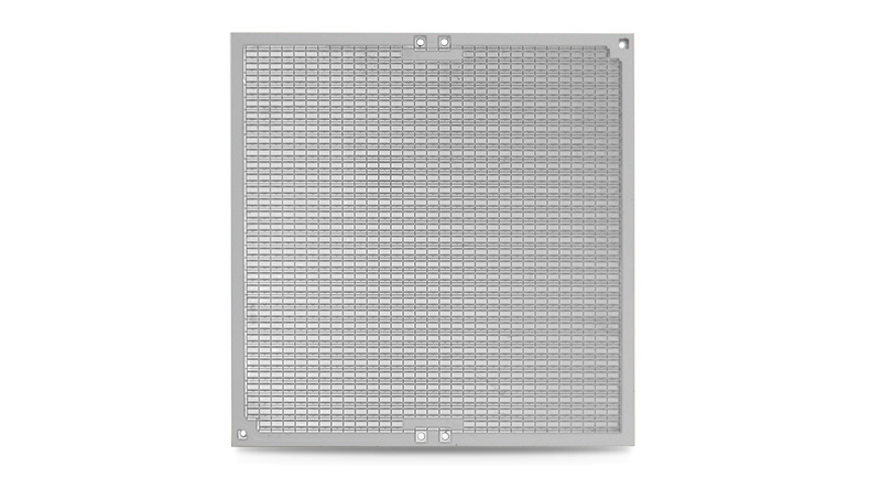
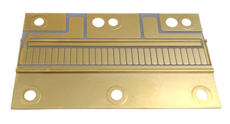 Multiple copper thickness on one layer
 Saphire Alumina 0.4mm 2 Layer Silver Conductor
 Alumina 0.5mm Silver Fin
Daleba can manufacture PCBs ranging from single-sided to complex boards in excess of 40x layers. Our in-house CAM engineering resource allows us to rapidly check, panelise and commercially optimise a fast turnaround prototype as well as small volumes. We can supply simple technology boards in as little as 24 hours!